| CPC H01L 31/022433 (2013.01) [H01L 31/02168 (2013.01); H01L 31/1864 (2013.01); H01L 31/184 (2013.01)] | 8 Claims |
|
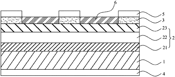
1. A manufacturing method of a solar cell, comprising:
forming an electricity generation layer on a substrate, including:
forming a back-surface field layer on the substrate,
forming a photovoltaic layer on the back-surface field layer, and
forming a window layer on the photovoltaic layer;
forming an ohmic contact layer on a surface of the electricity generation layer facing away from the substrate;
forming a back electrode on a surface of the substrate facing away from the electricity generation layer;
forming a top electrode on a surface of the ohmic contact layer facing away from the electricity generation layer using a printing process;
etching the ohmic contact layer with the top electrode as a mask to expose a partial region of the electricity generation layer;
forming an anti-reflection film over the partial region by sequentially stacking and forming Ti2O3 layer and a SiO2 layer on the partial region; and
wherein the substrate is made of an InP material.
|