| CPC H01L 29/7869 (2013.01) [H01L 29/4908 (2013.01); H01L 29/517 (2013.01); H01L 29/518 (2013.01); H01L 29/78648 (2013.01)] | 18 Claims |
|
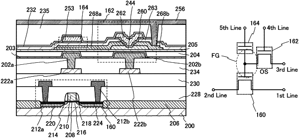
1. A semiconductor device comprising:
a first transistor;
a first insulating layer over the first transistor;
a second transistor over the first insulating layer; and
a capacitor electrically connected to the first transistor and the second transistor,
wherein the first transistor comprises:
a semiconductor layer comprising silicon;
a first gate insulating layer over the semiconductor layer;
a first gate electrode layer over the first gate insulating layer; and
a first source electrode layer and a first drain electrode layer over the semiconductor layer,
wherein the first insulating layer is provided over the first gate electrode layer and comprises silicon and nitrogen,
wherein the second transistor comprises:
a second gate electrode layer over the first insulating layer;
a second gate insulating layer over the second gate electrode layer;
an oxide semiconductor layer over the second gate insulating layer, the oxide semiconductor layer comprising In, Ga, and Zn,
a third gate insulating layer over the oxide semiconductor layer;
a third gate electrode layer over the third gate insulating layer; and
a second source electrode layer and a second drain electrode layer each having a region being in contact with a top surface of the oxide semiconductor layer,
wherein one of the second source electrode layer and the second drain electrode layer is electrically connected to the first gate electrode layer,
wherein a first electrode of the capacitor comprises a part of the one of the second source electrode layer and the second drain electrode layer,
wherein a second electrode of the capacitor comprises a first conductive layer provided over the one of the second source electrode layer and the second drain electrode layer, and
wherein a part of the first conductive layer overlaps with the first gate electrode layer.
|