| CPC H01L 29/78633 (2013.01) [G11C 19/28 (2013.01); H01L 29/66742 (2013.01)] | 18 Claims |
|
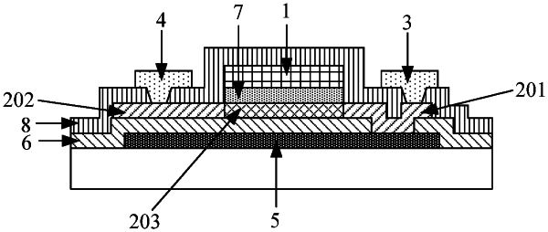
1. A thin film transistor, comprising:
at least one active layer pattern, the at least one active layer pattern comprises a first conductive pattern, a second conductive pattern, and a semiconductor pattern located between the first conductive pattern and the second conductive pattern;
a gate located on a side of the at least one active layer pattern and insulated from the at least one active layer pattern;
a first electrode and a second electrode, which are located on a side of the gate away from the at least one active layer pattern, and are respectively electrically connected with the first conductive pattern and the second conductive pattern;
a conductive shielding pattern is provided corresponding to the semiconductor pattern in the at least one active layer pattern, the conductive shielding pattern is located on a side of the semiconductor pattern away from the gate and is electrically connected with the first electrode, and a buffer layer is arranged between the conductive shielding pattern and the semiconductor pattern;
an orthographic projection of the conductive shielding pattern on a plane where the semiconductor pattern corresponding to the conductive shielding pattern is located at least partially covers the semiconductor pattern corresponding to the conductive shielding pattern, wherein the at least one active layer pattern includes a plurality of active layer patterns, and the plurality of active layer patterns are arranged in a first preset direction;
the gate, the first electrode, and the second electrode each extend along the first preset direction, the first electrode is electrically connected to first conductive patterns of the plurality of active layer patterns, and the second electrode is electrically connected to second conductive patterns of the plurality of active layer patterns.
|