|
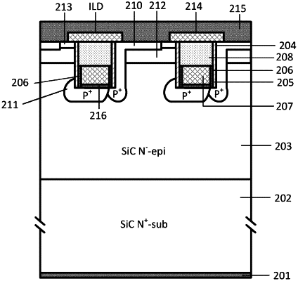
1. A trench gate silicon carbide metal oxide semiconductor field effect transistor (MOSFET) device, comprising a drain electrode located at a bottom of the device and a source electrode located at a top of the device, wherein a first conductive heavily doped silicon carbide substrate is disposed on the drain electrode; a first conductive lightly doped silicon carbide epitaxial layer is disposed on the first conductive heavily doped silicon carbide substrate; trench gates arranged periodically are provided on a surface of the first conductive lightly doped silicon carbide epitaxial layer; each of the trench gates comprises a gate dielectric layer disposed on a side wall of a trench, a conductive dielectric layer disposed above the trench, and a low-temperature oxide layer located below the trench; an insulating layer is disposed between the low-temperature oxide layer and the gate dielectric layer; a second conductive well region is disposed between the trench gates; an interlayer dielectric layer is disposed above the trench gate; one side edge of the trench gate is provided with a second conductive heavily doped side edge layer extending from a bottom corner of one side edge of the trench gate to an upper surface of the first conductive lightly doped silicon carbide epitaxial layer; a bottom corner of another side edge that is opposite to the bottom corner of one side edge of the trench gate is provided with a second conductive heavily doped bottom corner layer which is connected to the second conductive heavily doped side edge layer along a bottom of the trench gate through a layout design to obtain a same potential as the source electrode; a Schottky contact is formed between the bottom of the trench gate and the first conductive lightly doped silicon carbide epitaxial layer; ohmic contacts are formed between the bottom of the trench gate and the second conductive heavily doped bottom corner layer and between the bottom of the trench gate and the second conductive heavily doped side edge layer; a first conductive heavily doped source region is provided inside the second conductive well region and in a position adjacent to an upper surface of the second conductive heavily doped side edge layer; the interlayer dielectric layer covers part of the first conductive heavily doped source region; and the source electrode short-circuits the second conductive heavily doped side edge layer and the first conductive heavily doped source region.
|