| CPC H01L 29/66795 (2013.01) [H01L 21/0337 (2013.01); H01L 21/31053 (2013.01); H01L 21/31116 (2013.01); H01L 21/31144 (2013.01); H01L 21/32135 (2013.01); H01L 21/32139 (2013.01); H01L 21/823821 (2013.01); H01L 21/823828 (2013.01); H01L 29/401 (2013.01); H01L 29/66545 (2013.01); H01L 21/26513 (2013.01); H01L 21/823814 (2013.01); H01L 29/0847 (2013.01); H01L 29/6656 (2013.01)] | 20 Claims |
|
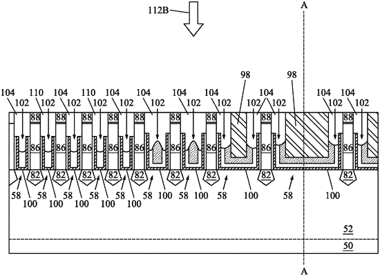
1. A method comprising:
forming a dielectric material over a source/drain region;
forming a first gate mask adjacent to the dielectric material and the source/drain region;
depositing a first filling layer over the first gate mask and the dielectric material;
depositing a second filling layer over the first filling layer;
planarizing the second filling layer with a chemical mechanical polish process, the chemical mechanical polish process being performed until the first filling layer is exposed; and
planarizing the first filling layer and remaining portions of the second filling layer with an etch-back process, the etch-back process etching materials of the first filling layer and the second filling layer at the same rate, wherein a top surface of the first filling layer is level with a top surface of the dielectric material after the etch-back process.
|