| CPC H01L 29/42392 (2013.01) [H01L 29/6656 (2013.01); H01L 29/78618 (2013.01); H01L 29/78696 (2013.01)] | 20 Claims |
|
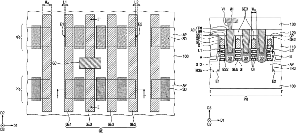
1. A semiconductor device, comprising:
an active pattern on a substrate, wherein the active pattern includes a plurality of channel layers that are stacked on one another and spaced apart from each other;
a plurality of source/drain patterns that are spaced apart from each other in a first direction and are disposed on the active pattern, wherein the plurality of source/drain patterns are connected to each other through the plurality of channel layers; and
first and second gate electrodes that at least partially surround the channel layers and extend in a second direction while extending across the active pattern, wherein the first and second gate electrodes are disposed adjacent to the plurality of source/drain patterns, wherein the second direction intersects the first direction,
wherein the active pattern has a first sidewall and a second sidewall that faces the first sidewall, and
wherein a first distance between the first sidewall of the active pattern and an outer sidewall of the first gate electrode is different from a second distance between the second sidewall of the active pattern and an outer sidewall of the second gate electrode.
|
|
11. A semiconductor device, comprising:
an active pattern on a substrate, wherein the active pattern includes a plurality of channel layers that are stacked and spaced apart from each other;
a plurality of source/drain patterns spaced apart from each other in a first direction and disposed on the active pattern, wherein the plurality of source/drain patterns are connected to each other through the channel layers; and
first to third gate electrodes that at least partially surround the channel layers and extend in a second direction while extending across the active pattern, wherein the first to third gate electrode are disposed between the plurality of source/drain patterns, wherein the second direction intersects the first direction,
wherein the active pattern has a first sidewall and a second sidewall that faces the first sidewall,
wherein each of the first sidewall and the second sidewall has a curved shape that is rounded toward an adjacent one of the plurality of source/drain patterns,
wherein the first gate electrode is adjacent to the first sidewall,
wherein the second gate electrode is adjacent to the second sidewall,
wherein the third gate electrode is between the first gate electrode and the second gate electrode, and
wherein a first distance between the first sidewall and an outer sidewall of the first gate electrode is less than a second distance between the second sidewall and an outer sidewall of the second gate electrode.
|
|
17. A semiconductor device, comprising:
a plurality of active patterns on a substrate, wherein each of the active patterns includes a plurality of channel layers that are stacked and spaced apart from each other;
a plurality of source/drain patterns spaced apart from each other in a first direction and disposed on the plurality of active patterns, wherein the plurality of source/drain patterns are connected to each other through the plurality of channel layers;
first to third gate electrodes at least partially surrounding the channel layers and extending in a second direction across the plurality of active patterns, wherein the plurality of source/drain patterns are disposed between the first to third gate electrodes, wherein the second direction intersects the first direction;
a gate dielectric pattern between the first to third gate electrodes and the plurality of channel layers;
a plurality of first gate spacers vertically extending from a top surface of an uppermost one of the channel layers and covering sidewalls of each of the first to third gate electrodes;
a plurality of second gate spacers between the plurality of source/drain patterns and the first to third gate electrodes, wherein the plurality of second gate spacers vertically overlap the plurality of first gate spacers;
a plurality of gate capping patterns between the plurality of first gate spacers and on the first to third gate electrodes;
an interlayer dielectric layer covering sidewalls and top surfaces of the plurality of first gate spacers and top surfaces of the plurality of gate capping patterns;
a plurality of active contacts on opposite sides of each of the first to third gate electrodes, wherein the active contacts penetrate the interlayer dielectric layer and are connected to the plurality of source/drain patterns; and
a gate contact penetrating the interlayer dielectric layer to connect to one of the first to third gate electrodes,
wherein the plurality of active patterns are spaced apart from each other in the second direction by a first trench, and are spaced apart from each other in the first direction by a second trench,
wherein each of the plurality of active patterns has a first sidewall and a second sidewall that faces the first sidewall,
wherein each of the first sidewall and the second sidewall has a curved shape that is rounded toward an adjacent one of the plurality of source/drain patterns,
wherein the first gate electrode is adjacent to the first sidewall,
wherein the second gate electrode is adjacent to the second sidewall,
wherein the third gate electrode is between the first gate electrode and the second gate electrode, and
wherein a first distance between the first sidewall and an outer sidewall of the first gate electrode is less than a second distance between the second sidewall and an outer sidewall of the second gate electrode.
|