| CPC H01L 29/41791 (2013.01) [H01L 27/0688 (2013.01); H01L 27/0886 (2013.01)] | 19 Claims |
|
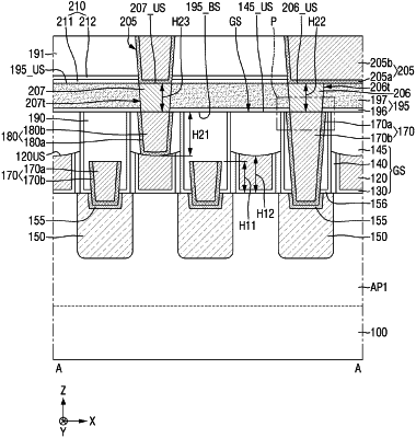
1. A semiconductor device comprising:
a gate structure on a substrate and including a gate electrode;
a gate contact connected to the gate electrode;
a source/drain pattern on a side surface of the gate electrode;
a source/drain contact connected to the source/drain pattern;
a first etching stop film structure on the source/drain contact and the gate structure, the first etching stop film structure including a first lower etching stop film and a silicon nitride film on the first lower etching stop film; and
a first via plug placed inside the first etching stop film structure and connected to the source/drain contact;
a second via plug in the first etching stop film structure and contacting an upper surface of the gate contact,
wherein the source/drain contact is between the source/drain pattern and the first via plug,
wherein the first lower etching stop film includes aluminum, and
wherein an upper surface of the silicon nitride film is on a same plane as an upper surface of the first via plug.
|