| CPC H01L 29/41775 (2013.01) [H01L 21/02123 (2013.01); H01L 21/02126 (2013.01); H01L 21/02167 (2013.01); H01L 21/02362 (2013.01); H01L 21/76829 (2013.01); H01L 21/76832 (2013.01); H01L 21/76834 (2013.01); H01L 29/0665 (2013.01); H01L 29/42392 (2013.01); H01L 29/78696 (2013.01)] | 18 Claims |
|
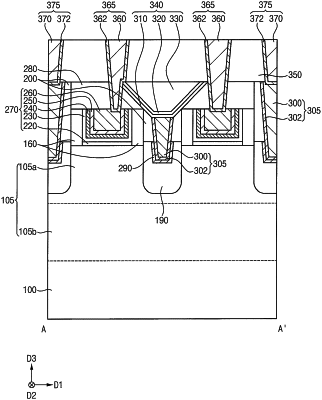
1. A semiconductor device, comprising:
a gate structure disposed on a substrate;
a source and drain layer disposed on the substrate adjacent the gate structure;
a first contact plug disposed on the source and drain layer;
an insulation pattern structure disposed on the first contact plug, the insulation pattern structure including insulation patterns having different carbon concentrations; and
a second contact plug disposed on the gate structure,
wherein the insulation pattern structure comprises a first insulation pattern, a second insulation pattern, and a third insulation pattern sequentially stacked in a vertical direction substantially perpendicular to an upper surface of the substrate,
wherein the second contact plug is in contact with upper surfaces of the first insulation pattern and the second insulation pattern, and
wherein a dielectric constant of the second insulation pattern is greater than a dielectric constant of the first insulation pattern, based on a carbon concentration of the second insulation pattern being greater than a carbon concentration of the first insulation pattern.
|