| CPC H01L 29/41775 (2013.01) [H01L 27/0886 (2013.01); H01L 29/7851 (2013.01)] | 18 Claims |
|
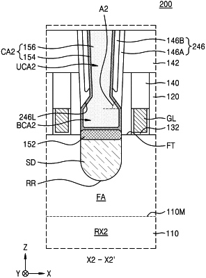
1. An integrated circuit device comprising:
a fin-type active region extending in a first lateral direction on a substrate;
a gate line extending in a second lateral direction, the gate line being on the fin-type active region, the second lateral direction intersecting with the first lateral direction;
an insulating spacer covering a sidewall of the gate line;
a source/drain region connected to the fin-type active region adjacent to the gate line and spaced apart from the insulating spacer, the source/drain region having a dopant profile different from a dopant profile of the fin-type active region;
a metal silicide film covering a top surface of the source/drain region; and
a source/drain contact apart from the gate line with the insulating spacer therebetween in the first lateral direction, the source/drain contact being connected to the source/drain region through the metal silicide film,
the source/drain contact including a bottom contact segment and an upper contact segment, the bottom contact segment having a contact surface in contact with a top surface of the metal silicide film, the upper contact segment being apart from the metal silicide film with the bottom contact segment therebetween in a vertical direction, the upper contact segment being integrally connected to the bottom contact segment, wherein a width of the bottom contact segment is greater than a width of at least a portion of the upper contact segment in the first lateral direction,
the metal silicide film contacting the insulating spacer and a region of the fin-type active region having the dopant profile of the fin-type active region.
|
|
12. An integrated circuit device comprising:
a fin-type active region extending in a first lateral direction on a substrate;
a recess region defined by the fin-type active region;
a pair of gate lines apart from each other with the recess region therebetween, the pair of gate lines extending in a second lateral direction on the fin-type active region, the second lateral direction intersecting with the first lateral direction;
a pair of insulating spacers covering sidewalls of each of the pair of gate lines;
a source/drain region in the recess region, connected to the fin-type active region adjacent to the gate line and spaced apart from the pair of insulating spacers, the source/drain region having a dopant profile different from a dopant profile of the fin-type active region;
a metal silicide film covering a top surface of the source/drain region; and
a source/drain contact between the pair of gate lines, the source/drain contact being connected to the source/drain region through the metal silicide film, the source/drain contact including a bottom contact segment and an upper contact segment, the bottom contact segment having a contact surface in contact with a top surface of the metal silicide film, the upper contact segment being apart from the metal silicide film with the bottom contact segment therebetween in a vertical direction, the upper contact segment being integrally connected to the bottom contact segment, a width of the bottom contact segment is greater than a width of at least a portion of the upper contact segment in the first lateral direction,
the metal silicide film contacting the pair of insulating spacers and a region of the fin-type active region having the dopant profile of the fin-type active region.
|