| CPC H01L 29/1054 (2013.01) [H01L 29/2003 (2013.01); H01L 29/42364 (2013.01); H01L 29/66446 (2013.01); H01L 29/7311 (2013.01); H01L 29/7827 (2013.01); H01L 29/7831 (2013.01)] | 20 Claims |
|
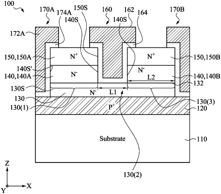
1. A method, comprising:
forming a first semiconductor layer of a first III-V compound semiconductor material over a substrate, the first semiconductor having a first conductivity type;
forming a second semiconductor layer over the first semiconductor layer, the second semiconductor layer having a first portion and a second portion adjacent to the first portion, the second portion having a second III-V compound semiconductor material;
forming a vertical stack of semiconductor layers over the first portion of the second semiconductor layer, the vertical stack including a third semiconductor layer and a fourth semiconductor layer stacked over the third semiconductor layer, the third semiconductor layer having a same second III-V compound semiconductor material as the second portion of the second semiconductor layer but with a different material composition, the fourth semiconductor layer having a second conductivity type;
forming a first gate structure over the second portion of the second semiconductor layer, the first gate structure in contact with a first sidewall of the third semiconductor layer; and
forming a second gate structure over the first semiconductor layer, the second gate structure in contact with a second sidewall of the third semiconductor layer from a first direction and in direct contact with the first semiconductor layer from a second direction different from the first direction.
|