| CPC H01L 29/1029 (2013.01) [H01L 21/8221 (2013.01); H01L 27/0688 (2013.01); H01L 27/1225 (2013.01); H01L 27/127 (2013.01); H01L 29/42392 (2013.01); H01L 29/66969 (2013.01)] | 20 Claims |
|
1. A structure, comprising:
a stacked strip structure, comprising:
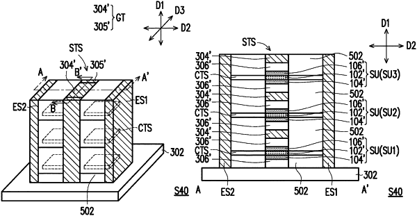
a first stacked unit, wherein the first stacked unit comprises a first channel layer and passivation layers covering a top surface and a bottom surface of the first channel layer;
a second stacked unit, wherein the second stacked unit is disposed on the first stacked unit and includes a second channel layer and passivation layers covering a top surface and a bottom surface of the second channel layer;
a gate structure wrapping around the first stacked unit and the second stacked unit, wherein two opposing sidewalls of the first channel layer and two opposing sidewalls of the second channel layer are exposed by the gate structure, and exposed from the stacked strip structure;
electrode strips located on two opposing sides of the stacked strip structure; and
a plurality of contact structures joining the first channel layer to the electrode strips, and joining the second channel layer to the electrode strips.
|