| CPC H01L 29/0649 (2013.01) [H01L 21/3065 (2013.01); H01L 21/31053 (2013.01); H01L 21/32139 (2013.01); H01L 21/762 (2013.01); H01L 21/764 (2013.01); H01L 21/76805 (2013.01); H01L 21/7682 (2013.01); H01L 21/76829 (2013.01); H01L 21/76889 (2013.01); H01L 21/823475 (2013.01); H01L 23/485 (2013.01); H01L 23/53266 (2013.01); H01L 23/5329 (2013.01); H01L 23/535 (2013.01); H01L 27/088 (2013.01); H01L 29/4975 (2013.01); H01L 21/31056 (2013.01); H01L 21/32 (2013.01); H01L 21/76849 (2013.01); H01L 21/76897 (2013.01); H01L 29/0653 (2013.01); H01L 29/161 (2013.01); H01L 29/401 (2013.01); H01L 29/41783 (2013.01); H01L 29/4991 (2013.01)] | 19 Claims |
|
1. A method of forming a semiconductor structure comprising:
providing parallel adjacent gate structures on a substrate, the parallel adjacent gate structures comprising an outer gate structure and an inner gate structure, wherein each of the parallel adjacent gate structures comprises a metal gate and a dielectric gate cap;
providing conductive trenches on opposite sides of the inner gate structure;
providing a first oxide layer on the dielectric gate caps;
providing contact area elements in the first oxide layer, wherein:
each of the contact area elements contacts one of the conductive trenches; and
upper surfaces of the contact area elements are substantially co-planar with an upper surface of the first oxide layer,
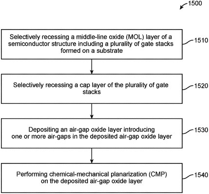
etching exposed portions of the first oxide layer to expose the dielectric gate caps;
recessing the exposed dielectric gate caps; and
depositing a second oxide layer to form airgaps, wherein portions of the airgaps are disposed in regions where the dielectric gate caps were recessed.
|