| CPC H01L 27/156 (2013.01) | 13 Claims |

|
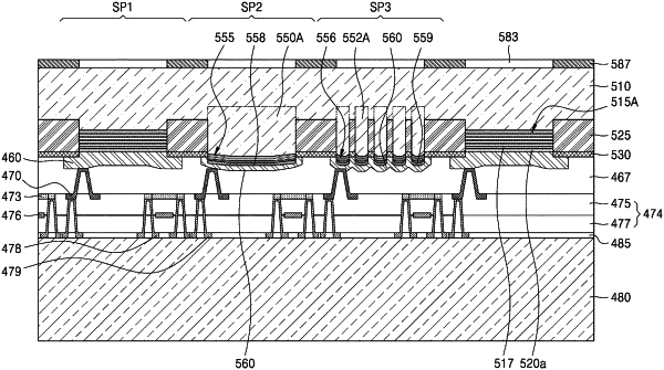
1. A method of manufacturing a micro light-emitting display apparatus, the method comprising:
forming a first active layer on a first semiconductor layer;
forming a second semiconductor layer on the first active layer;
forming a first isolation structure and a second isolation structure in the first active layers, the first isolation structure having a first width and the second isolation structure having a second width greater than the first width;
forming a first layer on the first active layer, the first isolation structure, and the second isolation structure;
exposing a first area of the second isolation structure;
forming a regrowth area by etching the exposed first area of the second isolation structure;
regrowing a semiconductor layer in the regrowth area;
planarizing the semiconductor layer to form a rod semiconductor layer;
forming a second active layer on the rod semiconductor layer; and
forming a third semiconductor layer on the second active layer.
|