| CPC H01L 27/156 (2013.01) [G09F 9/33 (2013.01); H01L 25/0753 (2013.01); H01L 25/167 (2013.01); H01L 33/382 (2013.01); H01L 33/62 (2013.01)] | 21 Claims |
|
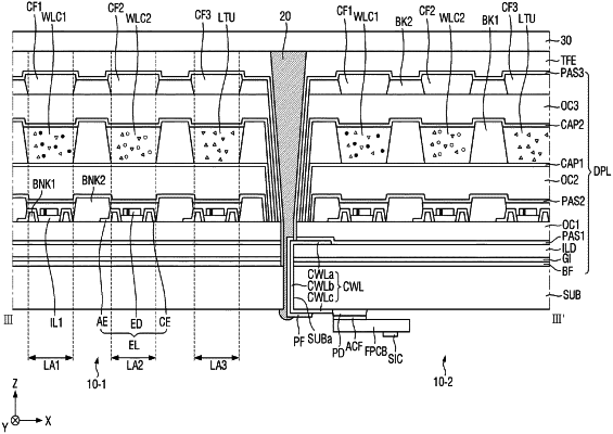
1. A tiled display device, comprising:
a plurality of display devices each including a display area and a non-display area adjacent to the display area, the display area of each of the plurality of display devices including a pixel; and
a substrate on which each of the plurality of display devices is disposed, wherein
each of the plurality of display devices comprises:
a thin film transistor layer disposed on the substrate and including a thin film transistor; and
a connection line electrically connected to the thin film transistor and disposed in the non-display area on the substrate, and
the connection line comprises:
a first portion electrically connected to the thin film transistor and disposed on the thin film transistor layer;
a second portion electrically connected to the first portion and disposed on a side surface of the substrate; and
a third portion electrically connected to the second portion and disposed on a lower surface of the substrate, and
the second portions of connection lines of display devices adjacent to each other among the plurality of display devices are staggered with respect to each other.
|