| CPC H01L 27/14641 (2013.01) [H01L 31/107 (2013.01); H01L 27/14623 (2013.01); H01L 27/14643 (2013.01)] | 20 Claims |
|
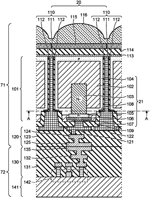
1. A solid-state image sensor comprising:
a semiconductor substrate including a first trench provided on a first surface and a second trench provided along a bottom portion of the first trench; and
a photoelectric conversion element provided on the semiconductor substrate,
wherein the photoelectric conversion element includes
a photoelectric conversion region provided in an element region partitioned by the first trench and the second trench in the semiconductor substrate and photoelectrically converting incident light to generate a charge,
a first semiconductor region surrounding the photoelectric conversion region in the element region,
a first contact in contact with the first semiconductor region at the bottom portion of the first trench,
a first electrode in contact with the first contact in the first trench,
a second semiconductor region provided in a region in the element region in contact with the first semiconductor region and having a first conductive type, which is an equal type to that of the first semiconductor region,
a third semiconductor region serving as a region in the element region in contact with the second semiconductor region, provided between the second semiconductor region and the first surface, and having a second conductive type, which is an opposite type to that of the first conductive type,
a second contact provided on the first surface so as to be in contact with the third semiconductor region, and
a second electrode in contact with the second contact, and
a second surface at which the first contact and the first electrode are in contact with each other is inclined with respect to the first surface.
|