| CPC H01L 27/14636 (2013.01) [H01L 27/14605 (2013.01); H01L 27/14609 (2013.01); H01L 27/14641 (2013.01); H01L 27/14643 (2013.01); H01L 27/14645 (2013.01); H01L 27/14647 (2013.01); H01L 27/14649 (2013.01); H01L 27/14652 (2013.01); H01L 27/14687 (2013.01); H01L 27/14689 (2013.01); H01L 25/043 (2013.01); H01L 25/0657 (2013.01); H01L 25/167 (2013.01); H01L 25/50 (2013.01)] | 11 Claims |
|
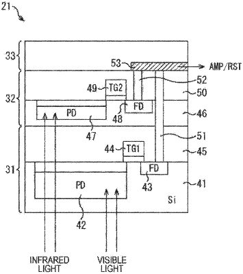
1. A light detecting device, comprising:
a first semiconductor layer in which a first photoelectric conversion unit and a first floating diffusion are disposed;
a second semiconductor layer in which a second photoelectric conversion unit and a second floating diffusion are disposed;
a wiring layer including a wiring electrically connected to the first and second floating diffusions, wherein
the first semiconductor layer and the second semiconductor layer are laminated with each other,
the wiring layer is formed on a side of the first or the second semiconductor layer, the side being opposite to a side on which the first semiconductor layer and the second semiconductor layer face each other, and
one of the first semiconductor layer and the second semiconductor layer is disposed between the wiring layer and the other of the first semiconductor layer and the second semiconductor layer, the one of the first semiconductor layer and the second semiconductor layer comprising a semiconductor material layer and an interlayer insulating film; and
a first wiring electrically connected to the wiring and one of the first floating diffusion and the second floating diffusion, the other of the first floating diffusion and the second floating diffusion being disposed between the wiring layer and the one of the first floating diffusion and the second floating diffusion and at least the first wiring being disposed in the semiconductor material layer.
|