| CPC H01L 27/1463 (2013.01) [H01L 27/14621 (2013.01); H01L 27/14627 (2013.01); H01L 27/14636 (2013.01)] | 20 Claims |
|
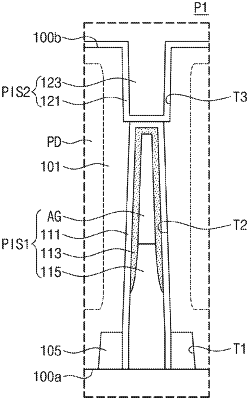
1. An image sensor, comprising:
a semiconductor substrate having a first surface and a second surface opposite to the first surface;
a first pixel isolation structure disposed in a first trench,
wherein the first trench vertically extends from the first surface of the semiconductor substrate and defines a plurality of pixel regions; and
a second pixel isolation structure disposed in a second trench,
wherein the second trench vertically extends from the second surface of the semiconductor substrate, and the second pixel isolation structure overlaps the first pixel isolation structure,
wherein the first pixel isolation structure comprises:
a liner semiconductor pattern,
wherein the liner semiconductor pattern defines a gap region in the first trench, and comprises a plurality of sidewall portions and a bottom portion connecting the sidewall portions;
a liner insulating pattern disposed between the liner semiconductor pattern and the semiconductor substrate; and
a capping insulating pattern disposed in the gap region of the liner semiconductor pattern.
|