| CPC H01L 27/14618 (2013.01) [H01L 27/14636 (2013.01); H01L 27/14683 (2013.01)] | 19 Claims |
|
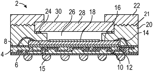
1. A semiconductor package comprising:
a substrate;
a die coupled to the substrate;
a glass lid coupled over the die, the glass lid comprising an inner surface facing the die, an outer surface opposite the inner surface, and a sidewall between the inner surface and the outer surface; and
a first molding compound and a second molding compound forming an interface around the glass lid;
wherein the first molding compound and the second molding compound are directly coupled to the sidewall of the glass lid.
|