| CPC H01L 27/14605 (2013.01) [H01L 27/14669 (2013.01); H04N 25/705 (2023.01); H04N 25/77 (2023.01)] | 8 Claims |
|
1. An imaging device comprising:
a semiconductor substrate;
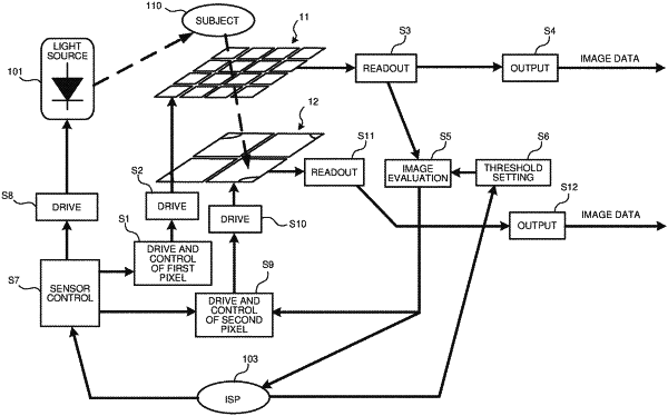
a first pixel array including a first light receiving pixel arranged above the semiconductor substrate, the first light receiving pixel having a stacked structure including a first electrode, a photoelectric conversion layer, and a second electrode that are sequentially stacked, the first light receiving pixel being configured to photoelectrically converts light in a first wavelength region including a visible light region;
a second pixel array including a second light receiving pixel arranged at a position overlapping the first light receiving pixel in the semiconductor substrate in a thickness direction of the semiconductor substrate, the second light receiving pixel being configured to photoelectrically converts light in a second wavelength region including an infrared light region;
a control unit configured to drive and control the second pixel array based on a signal photoelectrically converted by the first pixel array; and
a data processing unit configured to detect the first light receiving pixel having a change from image data captured by the first pixel array, wherein
the control unit performs control to output a signal photoelectrically converted by the second light receiving pixel corresponding to the first light receiving pixel having the change detected by the data processing unit.
|