| CPC H01L 27/14603 (2013.01) [H04N 25/77 (2023.01); H04N 25/78 (2023.01)] | 26 Claims |
|
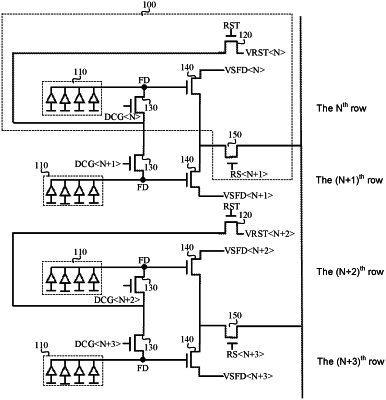
1. An image sensor, comprising:
a plurality of pixel blocks arranged in rows and columns, wherein each of the plurality of pixel blocks comprises:
a floating diffusion active region;
at least one photosensitive unit connected between the floating diffusion active region and a first reference voltage;
a reset transistor, wherein a control terminal of the reset transistor is connected to a reset control signal, and a second terminal of the reset transistor is connected to a reset voltage;
a gain control transistor, wherein a control terminal of the gain control transistor is connected to a gain control signal, a first terminal of the gain control transistor is connected to the floating diffusion active region, and a second terminal of the gain control transistor is connected to a first terminal of the reset transistor;
a source follower transistor, wherein a control terminal of the source follower transistor is connected to the floating diffusion active region, and a second terminal of the source follower transistor is connected to a following voltage; and
a select transistor, wherein a control terminal of the select transistor is connected to a select control signal, a first terminal of the select transistor outputs a pixel signal, and a second terminal of the select transistor is connected to a first terminal of the source follower transistor;
wherein two groups each composed of two adjacent pixel blocks in three adjacent pixel blocks in the same column share the same select transistor and the same reset transistor, respectively, and different pixel blocks comprise different floating diffusion active regions, and different source follower transistors.
|