| CPC H01L 27/1446 (2013.01) [H01L 31/1013 (2013.01)] | 7 Claims |
|
1. A detection device comprising
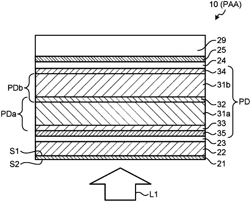
a plurality of optical sensors arranged on a substrate in first and second directions along a plane of the substrate which has a normal direction orthogonal to the plane of the substrate, wherein
each of the optical sensors comprises:
a first photodiode; and
a second photodiode that is coupled in series and in an opposite direction to the first photodiode, wherein
the first photodiode is stacked on the second photodiode in the normal direction,
the optical sensors are configured such that a first electrode, an electron transport layer, a first active layer, a hole transport layer, a second active layer, and a second electrode are stacked in the normal direction of the substrate in the order as listed,
the first active layer includes a p-n heterojunction of the first photodiode,
the second active layer includes a p-n heterojunction of the second photodiode,
the first active layer is in direct contact with the hole transport layer, and
the second active layer is in direct contact with the hole transport layer.
|