US 12,237,345 B2
Semiconductor device
Hajime Watakabe, Tokyo (JP); Isao Suzumura, Tokyo (JP); Akihiro Hanada, Tokyo (JP); and Yohei Yamaguchi, Tokyo (JP)
Assigned to Japan Display Inc., Tokyo (JP)
Filed by Japan Display Inc., Tokyo (JP)
Filed on Aug. 8, 2023, as Appl. No. 18/366,859.
Application 18/366,859 is a continuation of application No. 17/459,423, filed on Aug. 27, 2021, granted, now 11,764,233.
Application 17/459,423 is a continuation of application No. 16/852,925, filed on Apr. 20, 2020, granted, now 11,133,337, issued on Sep. 28, 2021.
Application 16/852,925 is a continuation of application No. PCT/JP2018/028405, filed on Jul. 30, 2018.
Claims priority of application No. 2017-207026 (JP), filed on Oct. 26, 2017.
Prior Publication US 2023/0387146 A1, Nov. 30, 2023
This patent is subject to a terminal disclaimer.
Int. Cl. H01L 27/12 (2006.01); H01L 29/24 (2006.01); H01L 29/66 (2006.01); H01L 29/786 (2006.01)
CPC H01L 27/1292 (2013.01) [H01L 27/1225 (2013.01); H01L 29/24 (2013.01); H01L 29/66757 (2013.01); H01L 29/66969 (2013.01); H01L 29/78666 (2013.01); H01L 29/7869 (2013.01)] 6 Claims
OG exemplary drawing
 
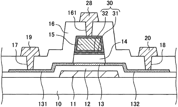
1. A semiconductor device comprising:
an oxide semiconductor film,
a gate electrode, and
a gate insulating film arranged between the oxide semiconductor film and the gate electrode,
wherein an aluminum oxide film is arranged between the gate insulating film and the gate electrode,
the aluminum oxide film has a first aluminum oxide film and a second aluminum oxide film,
the gate insulating film is made of silicon oxide,
a first oxygen concentration in the first aluminum oxide film is bigger than a second oxygen concentration in the second aluminum oxide film.