| CPC H01L 27/0922 (2013.01) [H01L 21/02603 (2013.01); H01L 21/28123 (2013.01); H01L 21/823807 (2013.01); H01L 21/823814 (2013.01); H01L 21/823828 (2013.01); H01L 21/823871 (2013.01); H01L 23/5286 (2013.01); H01L 29/0673 (2013.01); H01L 29/41733 (2013.01); H01L 29/42392 (2013.01); H01L 29/78618 (2013.01); H01L 29/78696 (2013.01)] | 6 Claims |
|
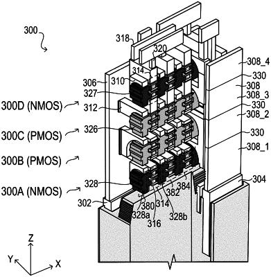
1. A semiconductor device, comprising:
a first transistor tier over a substrate, the first transistor tier being positioned in a first tier of the semiconductor device and including bottom transistors that are arranged along a horizontal direction parallel to the substrate, a first bottom transistor of the bottom transistors including a first bottom source/drain (S/D) region, a first bottom gate structure, and a second bottom S/D region that are arranged along the horizontal direction;
a first segment of a first conductive plane adjacent to a first side of the first transistor tier, the first segment of the first conductive plane being positioned over the substrate and disposed in the first tier, spanning a height of the first transistor tier, and connected to one of the first bottom S/D region and the second bottom S/D region of the first bottom transistor of the bottom transistors;
a second transistor tier over the first transistor tier, the second transistor tier being disposed in a second tier of the semiconductor device and including top transistors that are arranged along the horizontal direction, a first top transistor of the top transistors including a first top S/D region, a first top gate structure, and a second top S/D region that are arranged along the horizontal direction and; and
a second segment of the first conductive plane adjacent to a first side of the second transistor tier and in the second tier, the second segment of the first conductive plane being positioned over and connected to the first segment of the first conductive plane, and spanning a height of the second transistor tier.
|