US 12,237,328 B2
Minimizing shorting between FinFET epitaxial regions
Kangguo Cheng, Schenectady, NY (US); Balasubramanian Pranatharthiharan, Watervliet, NY (US); Alexander Reznicek, Troy, NY (US); and Charan V. Surisetty, Clifton Park, NY (US)
Assigned to Adeia Semiconductor Solutions LLC, San Jose, CA (US)
Filed by Adeia Semiconductor Solutions LLC, San Jose, CA (US)
Filed on Apr. 19, 2023, as Appl. No. 18/136,641.
Application 15/203,847 is a division of application No. 14/680,099, filed on Apr. 7, 2015, granted, now 9,443,853, issued on Sep. 13, 2016.
Application 18/136,641 is a continuation of application No. 17/175,340, filed on Feb. 12, 2021, granted, now 11,664,375.
Application 17/175,340 is a continuation of application No. 16/296,433, filed on Mar. 8, 2019, granted, now 10,923,471, issued on Feb. 16, 2021.
Application 16/296,433 is a continuation of application No. 15/923,097, filed on Mar. 16, 2018, granted, now 10,276,569, issued on Apr. 30, 2019.
Application 15/923,097 is a continuation of application No. 15/494,586, filed on Apr. 24, 2017, granted, now 9,985,024, issued on May 29, 2018.
Application 15/494,586 is a continuation of application No. 15/203,847, filed on Jul. 7, 2016, granted, now 9,704,753, issued on Jul. 11, 2017.
Prior Publication US 2024/0055426 A1, Feb. 15, 2024
This patent is subject to a terminal disclaimer.
Int. Cl. H01L 27/088 (2006.01); H01L 21/28 (2006.01); H01L 21/8234 (2006.01); H01L 21/8238 (2006.01); H01L 21/84 (2006.01); H01L 27/092 (2006.01); H01L 27/12 (2006.01); H01L 29/06 (2006.01); H01L 29/08 (2006.01); H01L 29/417 (2006.01); H01L 29/423 (2006.01); H01L 29/49 (2006.01); H01L 29/66 (2006.01); H01L 29/78 (2006.01); H10B 12/00 (2023.01)
CPC H01L 27/0886 (2013.01) [H01L 21/28035 (2013.01); H01L 21/28079 (2013.01); H01L 21/28088 (2013.01); H01L 21/823418 (2013.01); H01L 21/823431 (2013.01); H01L 21/823437 (2013.01); H01L 21/823481 (2013.01); H01L 21/823821 (2013.01); H01L 21/845 (2013.01); H01L 27/0924 (2013.01); H01L 27/1211 (2013.01); H01L 29/0649 (2013.01); H01L 29/0653 (2013.01); H01L 29/0847 (2013.01); H01L 29/41791 (2013.01); H01L 29/42376 (2013.01); H01L 29/4916 (2013.01); H01L 29/495 (2013.01); H01L 29/4966 (2013.01); H01L 29/66545 (2013.01); H01L 29/66795 (2013.01); H01L 29/785 (2013.01); H01L 29/7851 (2013.01); H01L 29/7855 (2013.01); H10B 12/056 (2023.02); H10B 12/36 (2023.02); H10B 12/37 (2023.02)] 16 Claims
OG exemplary drawing
 
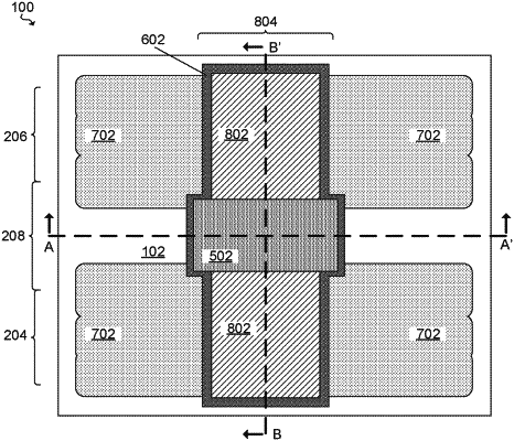
1. A structure comprising:
a first gate separated from a second gate by a dielectric region;
a first semiconductor fin associated with the first gate;
a second semiconductor fin associated with the second gate; and
a continuous spacer surrounding the first gate, the second gate, and the dielectric region, wherein:
the continuous spacer directly contacts vertical sidewalls of each of the first gate, the second gate, and the dielectric region;
the first gate and the second gate are aligned along a first direction and extend from opposite sides of the dielectric region;
widths of the first and second gates in a second direction are less than a width of the dielectric region in the second direction; and
the second direction is orthogonal to the first direction.