| CPC H01L 27/0605 (2013.01) [H01L 21/02181 (2013.01); H01L 21/02189 (2013.01); H01L 21/02194 (2013.01); H10B 12/315 (2023.02); H10B 12/482 (2023.02); H10B 12/485 (2023.02)] | 20 Claims |
|
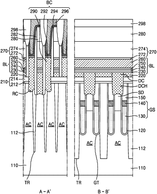
1. An integrated circuit device comprising:
a plurality of gate structures embedded in a substrate;
a direct contact on the substrate between the plurality of gate structures; and
a bit line electrode layer on the direct contact,
wherein the bit line electrode layer has a thickness of about 10 nm to 30 nm, and
the bit line electrode layer comprises a molybdenum tungsten (MoW) alloy including molybdenum (Mo) in a range of about 25 at % to about 75 at %.
|