| CPC H01L 27/0207 (2013.01) [H01L 21/28525 (2013.01); H01L 21/28568 (2013.01); H01L 21/823821 (2013.01); H01L 21/823871 (2013.01); H01L 23/522 (2013.01); H01L 23/5286 (2013.01); H01L 23/53209 (2013.01); H01L 23/53271 (2013.01); H01L 27/0924 (2013.01); H01L 29/41791 (2013.01); H01L 29/42356 (2013.01); H01L 29/42372 (2013.01); H01L 29/42376 (2013.01); H01L 29/4238 (2013.01); H01L 29/66795 (2013.01); H01L 29/7855 (2013.01); H01L 29/7856 (2013.01)] | 20 Claims |
|
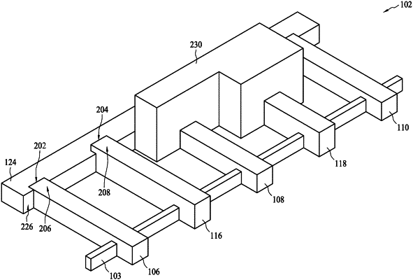
1. A semiconductor device, comprising:
a fin structure, disposed on a substrate;
a first conductive line, wrapping a first portion of the fin structure;
a second conductive line, attached on a second portion of the fin structure, the second portion being different from the first portion;
an isolation region, formed on the substrate and having a first side attached on one end of the second conductive line; and
a first conductive rail, disposed in a same layer as the first conductive line and the second conductive line on the substrate, the first conductive rail being attached on one end of the first conductive line and a second side of the isolation region opposite to the first side to be laterally contacted by the first conductive line and the isolation region.
|