| CPC H01L 25/18 (2013.01) [H01L 24/08 (2013.01); H01L 25/0657 (2013.01); H01L 2224/08146 (2013.01); H01L 2225/06513 (2013.01); H01L 2225/06541 (2013.01); H01L 2924/1431 (2013.01); H01L 2924/1436 (2013.01)] | 20 Claims |
|
1. A stacked-chip package, comprising:
a first stacked-chip package; and
a second stacked-chip package on the first stacked-chip package,
wherein each of the first stacked-chip package and second stack-chip package includes a first chip, and a second chip stacked on the first chip,
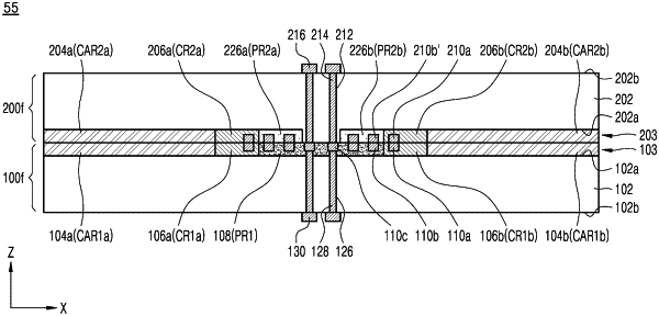
wherein the first chip includes a first cell array region, a first core circuit region including a first core terminal, a first peripheral circuit region including a plurality of first peripheral circuit terminals, and a first through via connected to at least one first peripheral circuit terminal of the plurality of first peripheral circuit terminals, and
wherein the second chip includes a second cell array region on the first cell array region, a second core circuit region on the first core circuit region and including a second core terminal, and a second through via on the first peripheral circuit region and connected to at least one first peripheral circuit terminal of the plurality of first peripheral circuit terminals.
|