|
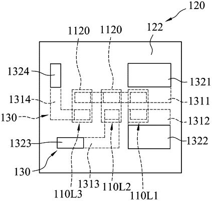
1. An LED device comprising: a plurality of LED chips, each of said LED chips having a first surface, a second surface opposite to said first surface, and a side surface that is connected between said first surface and said second surface, and including an electrode assembly disposed on said second surface, said first surface being a light exit surface; a first encapsulating sub-layer enclosing said side surface of each of said LED chips; an electric circuit layer assembly including a first electric circuit layer disposed on said second surface of each of said LED chips and said first encapsulating sub-layer, said first electric circuit layer including a first portion in contact with said electrode assembly of each of said LED chips and a second portion in direct contact with said first encapsulating sub-layer; and a second encapsulating sub-layer disposed on a portion of a top surface of said first electric circuit layer and enclosing said electric circuit layer assembly in such a manner that at least a portion of a surface of said second portion of said first electric circuit layer is exposed from said second encapsulating sub-layer.
|
