| CPC H01L 25/0753 (2013.01) [H01L 27/1214 (2013.01); H01L 33/007 (2013.01); H01L 33/0093 (2020.05); H01L 33/22 (2013.01); H01L 33/42 (2013.01); H01L 33/44 (2013.01); H01L 33/62 (2013.01); H01L 2933/0016 (2013.01); H01L 2933/0025 (2013.01)] | 10 Claims |
|
1. A method of manufacturing a light-emitting element, the method comprising:
providing a first substrate;
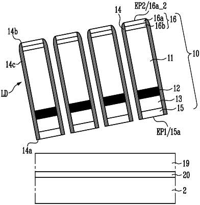
forming a light-emitting stack including a first electrode, a first semiconductor layer, an active layer, a second semiconductor layer, and a second electrode stacked on a first surface of the first substrate;
forming a buffer layer on the second electrode;
forming an adhesive layer on the buffer layer and arranging a second substrate on the adhesive layer to bond the first substrate and the second substrate;
turning the first substrate such that a second surface of the first substrate faces upward, the first surface and the second surface of the first substrate being opposite to each other;
removing the first substrate using a laser lift-off method to expose the first electrode;
etching the light-emitting stack in a vertical direction to form a light-emitting stack pattern and exposing a region of the buffer layer;
forming an insulating material layer on a surface of the light-emitting stack pattern and on the region of the buffer layer;
etching the insulating material layer in the vertical direction to form an insulating film surrounding the surface of the light-emitting stack pattern; and
separating the light-emitting stack pattern surrounded by the insulating film from the second substrate using a chemical lift-off method to form at least one light-emitting element, wherein
the at least one light-emitting element includes the second electrode, the second semiconductor layer, the active layer, the first semiconductor layer, and the first electrode disposed in a length direction of the at least one light-emitting element,
the first semiconductor layer includes an n-type semiconductor layer doped with an n-type dopant, and
the second semiconductor layer includes a p-type semiconductor layer doped with a p-type dopant.
|