| CPC H01L 25/0753 (2013.01) [F21K 9/232 (2016.08); H01L 23/5387 (2013.01); H01L 23/562 (2013.01); H01L 33/22 (2013.01); H01L 33/50 (2013.01); H01L 33/62 (2013.01); H01L 2933/0091 (2013.01)] | 20 Claims |
|
1. A light emitting device, comprising:
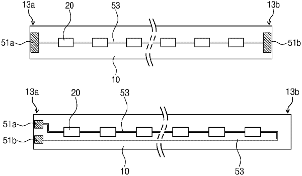
a substrate comprising a first surface and a second surface opposite to the first surface, the substrate extending in a first direction and having a width in a second direction;
a plurality of light emitting diodes disposed on the first surface of the substrate;
two electrode pads disposed on the substrate and including a first electrode pad and a second electrode pad;
a first solder and a second solder that include conductive materials and provided on a first terminal and a second terminal, respectively, the first terminal and the second terminal electrically coupled to electrodes of a light emitting diode;
a plurality of connection lines electrically connecting the plurality of light emitting diodes and the two electrode pads; and
an insulating layer disposed on the substrate to cover the plurality of light emitting diodes and including a first insulating layer and a second insulating layer,
wherein the plurality of connection lines includes a first connection line and a second connection line, and
wherein:
the first connection line connects at least two neighboring light emitting diodes among the plurality of light emitting diodes,
the second connection line connects the first electrode pad and a light emitting diode among the plurality of light emitting diodes which is positioned adjacent to the first electrode pad, and
the first insulating layer is provided only on a first region of the substrate without being disposed on a second region of the substrate, and wherein the first electrode pad and the second electrode pad are spaced apart from the first insulating layer, and
wherein the first terminal and the second terminal are attached, through the first solder and the second solder, to at least one of the first connection line or the second connection line that is disposed on the substrate.
|