| CPC H01L 25/0753 (2013.01) [H01L 33/382 (2013.01); H01L 33/56 (2013.01); H01L 33/62 (2013.01)] | 19 Claims |
|
1. A light-emitting diode (LED) packaging module, comprising:
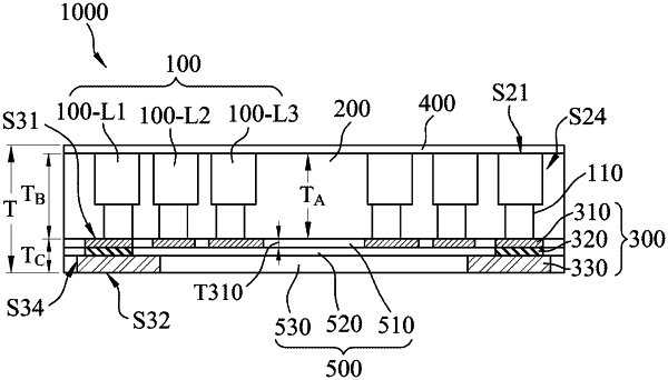
a plurality of LED chips that are spaced-apart from one another, each of said LED chips including:
a chip first surface as a light-exiting surface;
a chip second surface opposite to said chip first surface of said each of said LED chips;
a chip side surface that connects said chip first surface of said each of said LED chips and said chip second surface of said each of said LED chips; and
an electrode assembly disposed on said chip second surface of said each of said LED chips, said electrode assembly including a first electrode and a second electrode;
an encapsulating layer that covers said chip side surface of each of said LED chips and fills in a space among said LED chips, and that exposes said first electrode, said second electrode, and at least a portion of said chip first surface of each of said LED chips, said encapsulating layer being a colored layer;
a light-transmitting layer that is disposed on said encapsulating layer, that covers the portion of said chip first surface of each of said LED chips exposed from said encapsulating layer, and that has a light transmittance greater than that of said encapsulating layer;
a wiring assembly that is disposed on said chip second surface of each of said LED chips, that has a first wiring assembly surface connected to said electrode assembly of each of said LED chips, a second wiring assembly surface opposite to said first wiring assembly surface, and a side wiring assembly surface that is connected to said first wiring assembly surface and said second wiring assembly surface; and
an insulation component that covers said encapsulating layer and said wiring assembly,
wherein said LED chips are formed into a plurality of light-emitting units, each of said light-emitting units including at least three of said LED chips,
wherein said light-emitting units are arranged in an array having m row(s) and n column(s), m and n each independently representing a positive integer, and
wherein adjacent two of said light-emitting units are spaced apart from one another by a distance that is not greater than 1 mm.
|