| CPC H01L 25/0657 (2013.01) [H01L 25/50 (2013.01); H01L 2225/06513 (2013.01); H01L 2225/06541 (2013.01); H01L 2225/06586 (2013.01)] | 20 Claims |

|
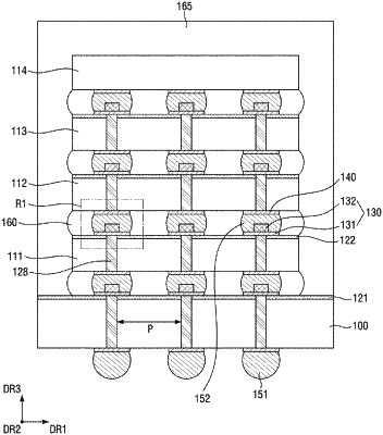
1. A semiconductor package comprising:
a first semiconductor chip having a first surface and a second surface opposite to the first surface, and including a first pad disposed on the first surface and a second pad disposed on the first surface, the first pad being spaced apart from the second pad; and
a second semiconductor chip having a third surface facing the first surface of the first semiconductor chip and a fourth surface opposite to the third surface, and including a third pad disposed beneath the third surface and a fourth pad disposed beneath the third surface, the third pad being spaced apart from the fourth pad,
wherein the first pad includes a first metal and a second metal, and the first metal is coupled to the third pad via the second metal,
the second pad is coupled to the fourth pad via a first solder ball, and
a width of the first solder ball is greater than a width of the second pad and a width of the fourth pad, respectively.
|