| CPC H01L 25/0657 (2013.01) [H01L 24/24 (2013.01); H01L 25/0652 (2013.01); H01L 25/105 (2013.01); H01L 25/18 (2013.01); H01L 24/08 (2013.01); H01L 2224/08145 (2013.01); H01L 2224/08235 (2013.01); H01L 2224/24227 (2013.01); H01L 2225/06517 (2013.01); H01L 2225/06544 (2013.01); H01L 2225/06548 (2013.01); H01L 2225/06555 (2013.01); H01L 2225/06568 (2013.01); H01L 2225/1035 (2013.01); H01L 2225/1058 (2013.01)] | 20 Claims |
|
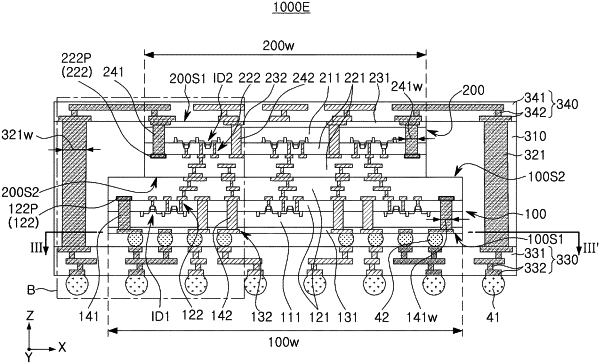
1. A method of manufacturing a semiconductor package, the method comprising:
forming a lower redistribution layer including a lower redistribution structure;
forming a conductive post on the lower redistribution layer, wherein the conductive post is electrically connected to the lower redistribution structure;
disposing a first semiconductor chip on the lower redistribution layer adjacent to the conductive post, wherein the first semiconductor chip includes a first circuit layer including a first circuit structure, and a first through via electrically connecting the first circuit layer and the lower redistribution structure to each other;
disposing a second semiconductor chip on the first semiconductor chip, wherein the second semiconductor chip includes a second circuit layer including a second circuit structure, and a second through via electrically connected to the second circuit layer, and wherein the second semiconductor chip is disposed on the first semiconductor chip such that the second circuit layer faces the first circuit layer;
forming an encapsulation layer covering at least a portion of each of the conductive post, the first semiconductor chip, and the second semiconductor chip; and
forming an upper redistribution layer on the encapsulation layer, wherein the upper redistribution layer includes an upper redistribution structure electrically connecting the second through via and the conductive post to each other,
wherein the first semiconductor chip receives power through the first through via, and the lower redistribution structure, and
wherein the second semiconductor chip receives power through the second through via, the upper redistribution structure, the conductive post, and the lower redistribution structure.
|