| CPC H01L 25/0657 (2013.01) [H01L 23/49816 (2013.01); H01L 24/05 (2013.01); H01L 24/48 (2013.01); H01L 24/49 (2013.01); H01L 24/73 (2013.01); H01L 2224/05552 (2013.01); H01L 2224/48091 (2013.01); H01L 2224/48135 (2013.01); H01L 2224/48227 (2013.01); H01L 2224/73265 (2013.01)] | 20 Claims |
|
1. A semiconductor package, comprising:
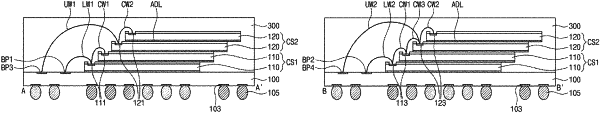
a package substrate including first bonding pads and second bonding pads that are alternately arranged in a single row along a first direction, third bonding pads that are spaced apart from the first bonding pads in a second direction intersecting the first direction, and fourth bonding pads that are spaced apart from the second bonding pads in the second direction;
a first chip stack including first chips that are stacked on the package substrate, each first chip including first signal pads and first power/ground pads that are alternately arranged in a single row along the first direction;
a second chip stack including second chips that are stacked on the first chip stack, each second chip including second signal pads and second power/ground pads that are alternately arranged in a single row along the first direction;
first lower wires that directly connect the first signal pads of one of the first chips to the first bonding pads;
second lower wires that directly connect the first power/ground pads of the one of the first chips to the second bonding pads;
first upper wires that directly connect the second signal pads of one of the second chips to the third bonding pads; and
second upper wires that directly connect the second power/ground pads of the one of the second chips to the fourth bonding pads,
wherein the first and second bonding pads are posed between the first chip stack and the third and fourth bonding pads, respectively.
|