| CPC H01L 25/0652 (2013.01) [H01L 25/18 (2013.01); H01L 2225/06506 (2013.01); H01L 2225/0651 (2013.01); H01L 2225/06517 (2013.01); H01L 2225/06562 (2013.01); H01L 2225/06575 (2013.01); H01L 2225/06586 (2013.01)] | 20 Claims |
|
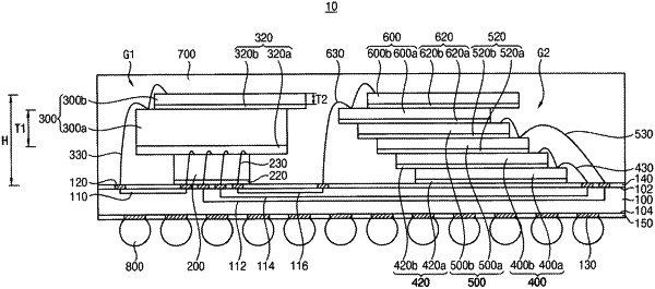
1. A semiconductor package, comprising:
a package substrate;
a processor chip mounted on the package substrate;
a first stack structure on the package substrate, the first stack structure including a number M of memory chips stacked on the processor chip, M being the number of all memory chips in the first stack structure; and
a second stack structure on the package substrate and spaced apart from the processor chip, the second stack structure including a number N of memory chips stacked on the package substrate, N being the number of all memory chips in the second stack structure,
wherein a number Q of channels that electrically connect the memory chips of the second stack structure with the processor chip and a number P of channels electrically connect the memory chips of the first stack structure with the processor chip,
wherein M, N, P, and Q are positive non-zero integers,
wherein the number N of all memory chips in the second stack structure is greater than the number M of all memory chips in the first stack structure,
wherein the semiconductor package contains a total number of memory chips that equals M+N,
wherein the processor chip is mounted on the package substrate in a flip chip bonding manner, and
wherein chip pads of the processor chip are electrically connected to the package substrate by conductive bumps.
|