| CPC H01L 24/27 (2013.01) [H01L 24/19 (2013.01); H01L 24/20 (2013.01); H01L 24/24 (2013.01); H01L 24/29 (2013.01); H01L 24/32 (2013.01); H01L 24/73 (2013.01); H01L 24/82 (2013.01); H01L 24/83 (2013.01); H01L 24/92 (2013.01); H01L 2224/211 (2013.01); H01L 2224/215 (2013.01); H01L 2224/24225 (2013.01); H01L 2224/2732 (2013.01); H01L 2224/27515 (2013.01); H01L 2224/29019 (2013.01); H01L 2224/29191 (2013.01); H01L 2224/32225 (2013.01); H01L 2224/73217 (2013.01); H01L 2224/82102 (2013.01); H01L 2224/82104 (2013.01); H01L 2224/83856 (2013.01); H01L 2224/83874 (2013.01); H01L 2224/9202 (2013.01); H01L 2224/92144 (2013.01); H01L 2924/3511 (2013.01)] | 14 Claims |
|
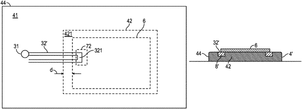
1. A method comprising:
disposing a layer of curable adhesive material on a substrate;
forming a pattern of microstructures on the layer of curable adhesive material;
curing a first region of the layer at a first level and a second region of the layer at a second level greater than the first level;
providing a solid circuit die to directly attach to a major surface of the first region of the layer; and
further curing the first region of the layer to anchor the solid circuit die on the first region by forming an adhesive bond therebetween.
|