| CPC H01L 24/20 (2013.01) [H01L 23/3121 (2013.01); H01L 24/13 (2013.01); H01L 24/29 (2013.01); H01L 24/73 (2013.01); H01L 25/0657 (2013.01); H01L 2224/73103 (2013.01)] | 20 Claims |
|
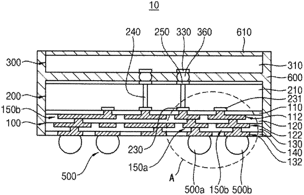
1. A semiconductor package comprising:
a first semiconductor chip including a first semiconductor substrate having a first surface and a second surface opposite to the first surface, a through electrode that extends through the first semiconductor substrate, a first chip pad on the first surface and electrically connected to a first end of the through electrode, and a second chip pad on the first surface and electrically connected to a circuit element in the first semiconductor substrate;
a redistribution wiring layer on and integrally with the first surface of the first semiconductor chip such that there is no space between the first surface of the first semiconductor substrate and the redistribution wiring layer, the redistribution wiring layer including a first redistribution wiring line electrically connected to the first chip pad and a second redistribution wiring line electrically connected to the second chip pad;
an insulation layer on the second surface of the first semiconductor substrate, the insulation layer having an upper surface that is planar across the second surface of the first semiconductor substrate;
a planar third chip pad in the insulation layer on the second surface of the first semiconductor substrate and electrically connected to a second end of the through electrode opposite the first end of the through electrode, the third chip pad having an upper surface that is exposed from the upper surface of the insulation layer, the upper surface of the third chip pad being coplanar with the upper surface of the insulation layer;
a second semiconductor chip stacked on the second surface of the first semiconductor chip, overlapping the first, second and third chip pads and the through electrode in a vertical direction, the second semiconductor chip electrically connected to the through electrode via the third chip pad and electrically isolated from the second redistribution wiring line;
an adhesive layer on an outer surface of the second semiconductor chip; and
a molding member on a side surface of the first semiconductor chip, a side surface of the redistribution wiring layer, a side surface of the second semiconductor chip, a side surface of the insulation layer and a side surface of the adhesive layer,
wherein the side surface of the redistribution wiring layer is coplanar with the side surface of the first semiconductor chip and the side surface of the second semiconductor chip.
|