| CPC H01L 24/08 (2013.01) [H01L 24/05 (2013.01); H01L 24/13 (2013.01); H01L 2224/0401 (2013.01); H01L 2224/05009 (2013.01); H01L 2224/05557 (2013.01); H01L 2224/08059 (2013.01); H01L 2224/13021 (2013.01); H01L 2924/35121 (2013.01)] | 20 Claims |
|
1. A semiconductor package comprising:
a semiconductor chip comprising a chip pad on a first surface of the semiconductor chip;
a first insulating layer arranged on the semiconductor chip, and comprising a first insulating hole exposing the chip pad and a second insulating hole spaced apart from the chip pad;
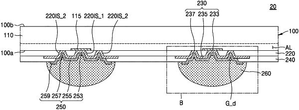
a redistribution pattern comprising a redistribution via pattern arranged on an internal surface of the first insulating layer that is configured to define the first insulating hole and on a surface of the chip pad, a redistribution dummy pattern arranged on an internal surface of the first insulating layer that is configured to define the second insulating hole and on the first surface of the semiconductor chip, and a redistribution line pattern arranged to extend on a surface of the first insulating layer in a horizontal direction and configured to connect the redistribution via pattern to the redistribution dummy pattern;
an under bump metal (UBM) comprising a first UBM portion arranged on the redistribution via pattern, a second UBM portion extending from the first UBM portion and arranged on the redistribution line pattern, and a UBM dummy portion extending from the second UBM portion and arranged on the redistribution dummy pattern; and
a connection terminal arranged on the UBM, and comprising a dummy portion configured to fill a dummy groove formed by the redistribution dummy pattern and the UBM dummy portion,
wherein the dummy portion of the connection terminal has a shape concavely protruding in a direction toward the first surface of the semiconductor chip.
|