| CPC H01L 23/60 (2013.01) [G01T 1/2018 (2013.01); H01L 27/14636 (2013.01); H01L 27/14663 (2013.01)] | 20 Claims |
|
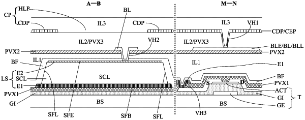
1. A sensing substrate, comprising:
a base substrate,
a first insulating layer;
a sensing unit on the base substrate, wherein the sensing unit comprises:
a sensing element located between the first insulating layer and the base substrate, wherein the sensing element has a light incident surface and a back surface that are opposite to each other and a side surface between the light incident surface and the back surface, the light incident surface is on a side of the back surface away from the base substrate; and
a conductive pattern on a side of the sensing element away from the base substrate, wherein the conductive pattern has a hollow portion and a transparent conductive portion surrounding the hollow portion, and an orthographic projection of the transparent conductive portion on the base substrate at least partially overlaps with an orthographic projection of the side surface of the sensing element on the base substrate.
|