| CPC H01L 23/60 (2013.01) [H10B 41/27 (2023.02); H10B 41/41 (2023.02); H10B 43/27 (2023.02); H10B 43/40 (2023.02)] | 12 Claims |
|
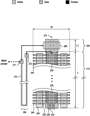
1. A semiconductor device, comprising:
a first active area extending in a first direction, wherein the first active area includes a first portion with a column of source contacts along the first direction and a second portion contiguous to the first portion;
a first gate over the second portion with a section of the second portion uncovered by the first gate, the section located away from the first portion and configured to couple with a ground node of the semiconductor device; and
a second active area located proximate to a side of the first active area, the second active area including at least one elongated segment extending in the first direction and first and second end portions of the second active area proximate to the second portion of the first active area, wherein the first and second end portions of the second active area are coupled with the first gate and the column of source contacts, respectively.
|