| CPC H01L 23/5286 (2013.01) [H01L 23/36 (2013.01); H01L 23/481 (2013.01); H01L 23/5226 (2013.01); H01L 24/08 (2013.01); H01L 2224/08145 (2013.01)] | 20 Claims |
|
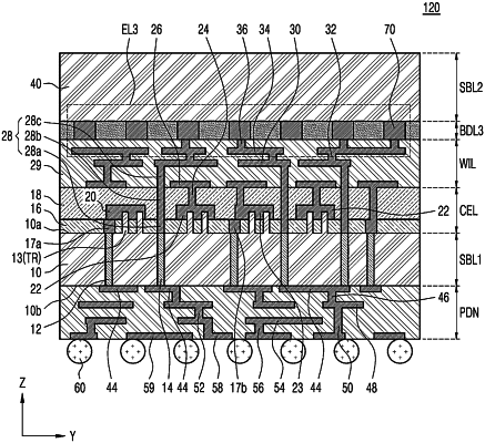
1. An integrated circuit semiconductor device comprising:
a substrate having a first surface and a second surface opposite the first surface;
a rail through via passing between the first surface and the second surface of the substrate;
a cell-level portion arranged on the first surface and including a buried rail connected to the rail through via, a local conductive interconnect, a cell via connected to the local conductive interconnect, and a transistor connected to the local conductive interconnect;
a signal wiring-level portion arranged on the cell-level portion and comprising an upper multi-layer interconnect layer connected to the local conductive interconnect via the cell via; and
a heat transfer line connected to the upper multi-layer interconnect layer and formed in the cell-level portion and the signal wiring-level portion.
|