| CPC H01L 23/528 (2013.01) [H01L 21/02172 (2013.01); H01L 21/02175 (2013.01); H01L 21/02181 (2013.01); H01L 21/76805 (2013.01); H01L 29/7869 (2013.01); H01L 29/78693 (2013.01); H10B 12/03 (2023.02); H10B 12/0335 (2023.02); H10B 12/315 (2023.02); H10B 12/34 (2023.02); H10B 12/48 (2023.02); H10B 12/482 (2023.02); H10B 12/485 (2023.02); H10B 12/50 (2023.02); H01L 21/76807 (2013.01); H10B 12/053 (2023.02)] | 20 Claims |

|
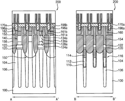
1. A method of manufacturing a semiconductor device, comprising:
forming a plurality of bit line structures in a cell region of a substrate;
forming a gate structure in core/peripheral regions of the substrate;
forming a lower contact plug and an upper contact plug between the bit line structures, wherein the lower contact plug and the upper contact plug are vertically stacked;
forming a capping insulation layer on a first bit line structure of the plurality of bit line structures, on the upper contact plug in the cell region, and on the gate structure in the core/peripheral regions;
forming a first photoresist pattern for forming landing pad patterns in the cell region and contact plugs in the core/peripheral regions on the capping insulation layer, wherein the first photoresist pattern is formed by performing a first exposure process;
etching layers using the first photoresist pattern as an etch mask to form first openings in the cell region and second openings in the core/peripheral regions;
forming a second photoresist pattern for forming wirings in the core/peripheral regions on the capping insulation layer, wherein the second photoresist pattern is formed by performing a second exposure process;
etching layers using the second photoresist pattern as an etch mask to form third openings in communication with the second openings in the core/peripheral regions; and
filling the first openings, the second openings, and the third openings with a first metal material to form the landing pad patterns in the first openings, the contact plugs in the second openings, and the wirings in the third openings.
|