| CPC H01L 23/5226 (2013.01) [H01L 21/561 (2013.01); H01L 21/563 (2013.01); H01L 23/3128 (2013.01); H01L 23/3171 (2013.01); H01L 23/481 (2013.01); H01L 23/5283 (2013.01); H01L 24/09 (2013.01); H01L 24/17 (2013.01); H01L 24/32 (2013.01); H01L 24/73 (2013.01); H01L 24/96 (2013.01); H01L 2224/02373 (2013.01); H01L 2224/02379 (2013.01); H01L 2224/02381 (2013.01); H01L 2224/0401 (2013.01); H01L 2224/73203 (2013.01)] | 20 Claims |
|
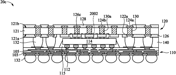
1. A semiconductor package, comprising:
an encapsulating layer;
a semiconductor die formed in the encapsulating layer; and
an interposer structure covering the encapsulating layer, comprising:
an insulating base having a first surface facing the encapsulating layer, and a second surface opposite the first surface;
a plurality of insulating features formed on the first surface of the insulating base and extending into the encapsulating layer, wherein the plurality of insulating features is arranged in a matrix which faces a top surface of the semiconductor die;
a plurality of first conductive features formed on the first surface of the insulating base and extending into the encapsulating layer, wherein the plurality of first conductive features surrounds the matrix of the plurality of insulating features; and
a plurality of first through-vias formed in the insulating base to be in direct contact with the plurality of the insulating features.
|