| CPC H01L 23/5226 (2013.01) [H01L 21/76846 (2013.01); H01L 21/7685 (2013.01); H01L 21/76883 (2013.01); H01L 23/5283 (2013.01); H01L 29/41725 (2013.01); H01L 29/456 (2013.01); H01L 21/76807 (2013.01); H01L 23/53209 (2013.01); H01L 23/53223 (2013.01); H01L 23/53238 (2013.01); H01L 23/53266 (2013.01)] | 20 Claims |
|
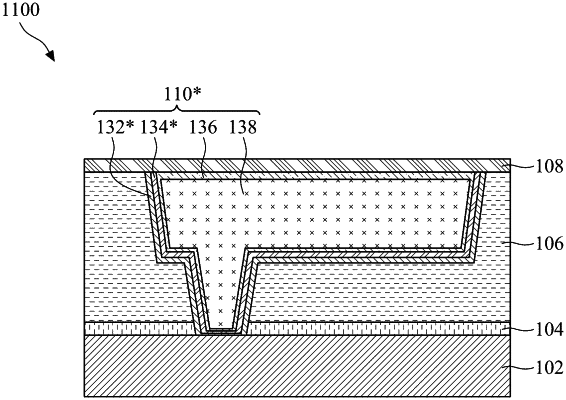
1. A semiconductor device comprising:
an insulating layer, wherein the insulating layer has a via opening and a conductive line opening;
a via in the via opening; and
a conductive line in the conductive line opening, wherein the conductive line comprises:
a first liner layer, wherein a first thickness of the first liner layer over the via is less than a second thickness of the first liner layer over the insulating layer, and
a conductive fill, wherein the first liner layer surrounds the conductive fill.
|