| CPC H01L 23/5225 (2013.01) [H01L 23/5286 (2013.01)] | 20 Claims |
|
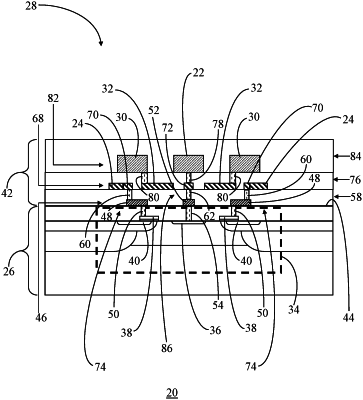
1. A method of forming a transistor comprising:
forming an interconnect structure on an upper surface of a semiconductor substrate having a first terminal and a second terminal,
the interconnect structure being formed of multiple layers of dielectric material and multiple layers of electrically conductive material; and
configuring the multiple layers of electrically conductive material to form, as parts of the interconnect structure:
a pillar in electrical contact with the first terminal;
a first runner electrically connected to the pillar;
a first tap interconnect in electrical contact with the second terminal;
a second runner electrically connected to the first tap interconnect;
a shield structure positioned between the pillar and the first tap interconnect; and
a shield runner electrically connected to the shield structure,
the shield runner overlying the second runner in a direction perpendicular to the upper surface of the semiconductor substrate.
|