| CPC H01L 23/49838 (2013.01) [H01L 21/4857 (2013.01); H01L 23/49816 (2013.01); H01L 23/49822 (2013.01); H01L 23/5383 (2013.01); H01L 23/5386 (2013.01); H01L 25/105 (2013.01); H01L 24/08 (2013.01); H01L 24/16 (2013.01); H01L 24/17 (2013.01); H01L 24/33 (2013.01); H01L 24/73 (2013.01); H01L 25/0652 (2013.01); H01L 25/18 (2013.01); H01L 2224/08225 (2013.01); H01L 2224/16227 (2013.01); H01L 2224/17181 (2013.01); H01L 2224/33181 (2013.01); H01L 2224/73204 (2013.01); H01L 2224/73253 (2013.01); H01L 2225/1035 (2013.01); H01L 2225/1058 (2013.01); H01L 2924/1431 (2013.01); H01L 2924/1433 (2013.01); H01L 2924/14361 (2013.01)] | 20 Claims |
|
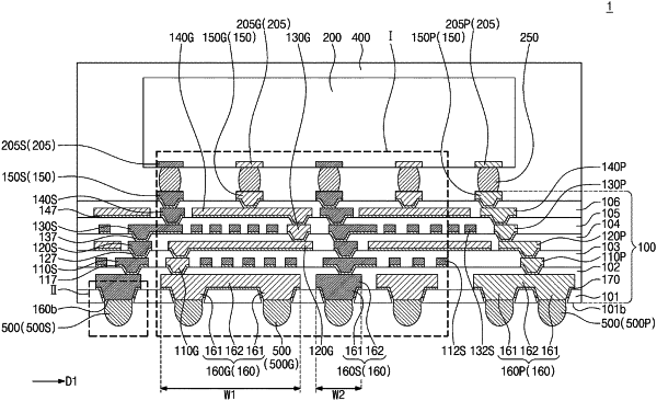
1. A semiconductor package, comprising:
a redistribution substrate that has a first surface and a second surface that face each other;
a semiconductor chip disposed on the first surface of the redistribution substrate; and
a plurality of solder patterns disposed on the second surface of the redistribution substrate,
wherein the redistribution substrate includes:
a first under-bump pattern; and
a plurality of second under-bump patterns that are laterally spaced apart from the first under-bump pattern,
wherein each of the first under-bump and the plurality of second under-bump patterns includes:
a first part coupled to one of the plurality of solder patterns; and
a second part formed on the first part and that is wider than the first part,
wherein the first part of the first under-bump pattern includes a plurality of first parts,
wherein the second part of the first under-bump pattern is connected to the plurality of the first parts of the first under-bump pattern,
wherein the redistribution substrate further includes an under-bump seed pattern that covers a sidewall of the first part and a bottom surface of the second part of the first under-bump and the plurality of second under-bump patterns, and
a dielectric layer that exposes a lowermost surface of the under-bump seed pattern.
|