| CPC H01L 23/49822 (2013.01) [H01L 23/49816 (2013.01); H01L 23/49838 (2013.01); H01L 24/08 (2013.01); H01L 24/16 (2013.01); H01L 24/32 (2013.01); H01L 24/73 (2013.01); H01L 25/0655 (2013.01); H01L 25/105 (2013.01); H01L 2224/08235 (2013.01); H01L 2224/16227 (2013.01); H01L 2224/16235 (2013.01); H01L 2224/32225 (2013.01); H01L 2224/73204 (2013.01); H01L 2225/1023 (2013.01); H01L 2225/1058 (2013.01); H01L 2924/15174 (2013.01)] | 20 Claims |
|
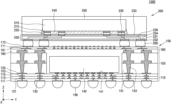
1. A semiconductor package comprising:
at least one first rewiring structure, the at least one first rewiring structure including a plurality of first insulating layers vertically stacked and a plurality of first patterned rewiring layers included in the plurality of first insulating layers;
at least one semiconductor chip on the at least one first rewiring structure; and
at least one molding layer covering the at least one semiconductor chip,
wherein each of the plurality of first patterned rewiring layers includes,
a first patterned conductive layer, the first patterned conductive layer including a curved upper surface, and
a first patterned seed layer covering a side surface and a lower surface of the first patterned conductive layer and having a conformal shape.
|