| CPC H01L 23/49816 (2013.01) [H01L 23/49838 (2013.01); H01L 24/48 (2013.01); H01L 2224/48229 (2013.01)] | 19 Claims |
|
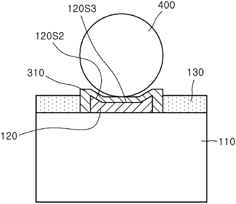
1. A semiconductor package comprising:
a package substrate;
a connection pad including a recessed portion disposed on one surface of the package substrate; and
an insulating pattern disposed on the one surface of the package substrate,
wherein the connection pad comprises:
an outer sidewall;
an inner sidewall in the recessed portion, the inner sidewall inclining in an inward direction from an upper portion; and
a groove pattern formed on the inner sidewall,
wherein the connection pad and the insulating pattern are spaced apart from each other by a distance in a lateral direction to form an empty space on the one surface of the package substrate.
|