| CPC H01L 23/49816 (2013.01) [H01L 23/293 (2013.01); H01L 23/49822 (2013.01); H01L 23/49838 (2013.01); H01L 23/5383 (2013.01); H01L 23/5386 (2013.01); H01L 24/16 (2013.01); H01L 24/32 (2013.01); H01L 24/73 (2013.01); H01L 25/0655 (2013.01); H01L 24/48 (2013.01); H01L 24/49 (2013.01); H01L 25/0657 (2013.01); H01L 25/105 (2013.01); H01L 2224/16235 (2013.01); H01L 2224/32225 (2013.01); H01L 2224/48145 (2013.01); H01L 2224/48227 (2013.01); H01L 2224/49109 (2013.01); H01L 2224/73204 (2013.01)] | 20 Claims |
|
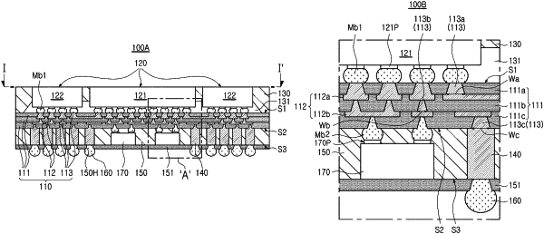
1. A semiconductor package, comprising:
a redistribution substrate having a first surface and a second surface opposite the first surface, and including a first insulating layer, a redistribution pattern disposed on the first insulating layer, and a redistribution via penetrating the first insulating layer and electrically connected to the redistribution pattern;
a first semiconductor chip disposed on the first surface of the redistribution substrate and electrically connected to the redistribution pattern;
a first encapsulant disposed on the first surface of the redistribution substrate and encapsulating at least a portion of the first semiconductor chip;
a passive device and a metal post disposed on the second surface of the redistribution substrate and electrically connected to the redistribution pattern;
a second encapsulant disposed on the second surface of the redistribution substrate and encapsulating at least side surfaces of the passive device and the metal post;
a second insulating layer disposed on a lower surface of the metal post and a lower surface of the second encapsulant, and having an opening exposing at least a portion of the lower surface of the metal post; and
a connection bump filling the opening of the second insulating layer and in direct contact with the lower surface of the exposed metal post,
wherein the metal post has a height greater than a height of each of the redistribution pattern and the redistribution via,
wherein the redistribution via includes a plurality of redistribution vias disposed on different levels,
wherein the plurality of redistribution vias include a first redistribution via connecting the first semiconductor chip to the redistribution pattern, a second redistribution via connecting the metal post to the redistribution pattern, and a third distribution via disposed between the first and second redistribution vias, and
wherein a maximum width of the first redistribution via a horizontal direction is greater than a maximum width of the third redistribution via in the horizontal direction.
|