| CPC H01L 23/49575 (2013.01) [H01L 21/4803 (2013.01); H01L 21/4828 (2013.01); H01L 23/3121 (2013.01); H01L 23/49558 (2013.01); H01L 23/49562 (2013.01); H01L 25/16 (2013.01); H01L 25/50 (2013.01); H02M 7/5387 (2013.01); H01L 24/32 (2013.01); H01L 24/40 (2013.01); H01L 24/92 (2013.01); H01L 2224/32245 (2013.01); H01L 2224/40139 (2013.01); H01L 2224/40245 (2013.01); H01L 2224/92246 (2013.01); H01L 2924/13091 (2013.01); H01L 2924/1426 (2013.01)] | 17 Claims |
|
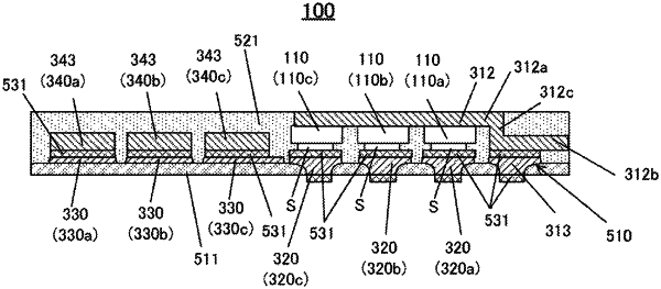
1. A semiconductor device comprising:
at least one first semiconductor element, each having a first electrode;
a second semiconductor element having a second electrode;
a first lead terminal connected to the first electrode of the at least one first semiconductor element;
a second lead terminal connected to the second electrode of the second semiconductor element;
a first resin with which the first lead terminal and the second lead terminal are held;
a second resin with which the at least one first semiconductor element and the second semiconductor element are sealed; and
a connecting conductor held by the first resin,
wherein the at least one first semiconductor element has a third electrode,
wherein the second semiconductor element has a fourth electrode, and
wherein the third electrode of the at least one first semiconductor element and the fourth electrode of the second semiconductor element are each connected to the connecting conductor,
wherein the first lead terminal and the second lead terminal each have a lower surface at a side opposite to a side where the at least one first semiconductor element and the second semiconductor element are arranged, at least a portion of each of the lower surfaces being exposed from the first resin,
wherein the first electrode and the third electrode of the first semiconductor element are arranged at a lower side of the first semiconductor element facing the first resin, and
wherein the second electrode and the fourth electrode of the second semiconductor element are arranged at a lower side of the second semiconductor element facing the first resin.
|